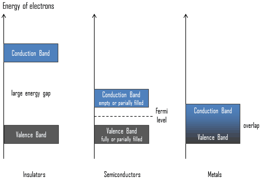
 In general, semiconductors are materials, inorganic or organic, which have the ability to control their conduction depending on chemical structure, temperature, illumination, and presence of dopants. The name semiconductor comes from the fact that these materials have an electrical conductivity between that of a metal, like copper, gold, etc. and an insulator, such as glass. They have an energy gap less than 4eV (about 1eV). In solid-state physics, this energy gap or band gap is an energy range between valence band and conduction band where electron states are forbidden. In contrast to conductors, electrons in a semiconductor must obtain energy (e.g. from ionizing radiation) to cross the band gap and to reach the conduction band.
Excitation by Ionizing Radiation
Energy for the excitation can be obtained by different ways. Electrons may reach the conduction band, when they are excited by ionizing radiation (i.e. they must obtain energy higher than Egap). In general, heavy charged particles transfer energy mostly by:
- Excitation. The charged particle can transfer energy to the atom, raising electrons to a higher energy levels.
- Ionization. Ionization can occur, when the charged particle have enough energy to remove an electron. This results in a creation of ion pairs in surrounding matter.
A convenient variable that describes the ionization properties of surrounding medium is the stopping power. The classical expression that describes the specific energy loss is known as the Bethe formula. For alpha particles and heavier particles the stopping power of most materials is very high for heavy charged particles and these particles have very short ranges.
In addition to these interactions, beta particles also lose energy by radiative process known as the bremsstrahlung. From classical theory, when a charged particle is accelerated or decelerated, it must radiate energy and the deceleration radiation is known as the bremsstrahlung (“braking radiation”).
Photons (gamma rays and X-rays) can ionize atoms directly (despite they are electrically neutral) through the Photoelectric effect and the Compton effect, but secondary (indirect) ionization is much more significant. Although a large number of possible interactions are known, there are three key interaction mechanisms with matter.
In all cases, a particle of ionizing radiation deposits a portion of its energy along its path. Particle passing through the detector ionizes the atoms of semiconductor, producing the electron-hole pairs. For example, typical thickness of silicon detector is about 300 µm so the number of generated electron-hole pairs by minimum ionizing particle (MIP) passing perpendicular through the detector is about 3.2 x 10⁴. This value is minor in comparison the total number of free carriers in intrinsic semiconductor of a surface of 1 cm2 and the same thickness. Note that, a sample of pure germanium at 20 °C contains about 1.26×10²¹ atoms, but also contains 7.5 x 10¹¹ free electrons and 7.5 x 10¹¹ holes constantly generated from thermal energy. As can be seen, the signal to noise ratio (S/N) would be minimal. The addition of 0.001% of arsenic (an impurity) donates an extra 1015 free electrons in the same volume and the electrical conductivity is increased by a factor of 10,000. In doped material the signal to noise ratio (S/N) would be even smaller. Cooling of the semiconductor is one way to lower this ratio.
Improvement can be reached by use of a reverse-bias voltage to the P-N junction to deplete the detector of free carriers, which is the principle of the most silicon radiation detectors. In this case, negative voltage is applied to the p-side and positive to the second one. Holes in the p-region are attracted from the junction towards the p contact and similarly for electrons and the n contact.
We hope, this article, Excitation by Ionizing Radiation, helps you. If so, give us a like in the sidebar. Main purpose of this website is to help the public to learn some interesting and important information about radiation and dosimeters.